This tutorial explained in detail everything inside the flip-flop, a fundamental building block in digital IC design, including the flip-flop's schematic and how it works.
Why Flip-Flop Understanding is Needed?
Flip-flop, which is typically used for data storage (D-type Flip-Flop), is one of the most critical components in any digital system. Understanding flip-flops will help designers understand the setup and hold time concepts, which are two of the most critical timing requirements that all the digital chips should meet before sending out for fabrication. Flip-flop's setup and hold time are also one of the most common interview questions for IC design engineers.
Below is a typical architecture of any sequential systems in digital IC/FPGA design involving 2 flip-flops (highlighted in red color) and the combinational logic.

Many flip-flops together form register banks. In microcontroller chips, registers typically store configuration data so that users can configure and change the chip functionalities using firmware.
Flip-flop Schematic
Below is the schematic of a flip-flop, which is widely used in the digital standard cell library for chip synthesis. For simplicity, a flip-flop without a reset pin is shown with data input (D), clock input (CK), and data output (Q). This is a rising-edge-triggered flip-flop.

The flip-flop schematic comprises one master latch and one slave latch. Each latch includes two transmission gates and three inverters.
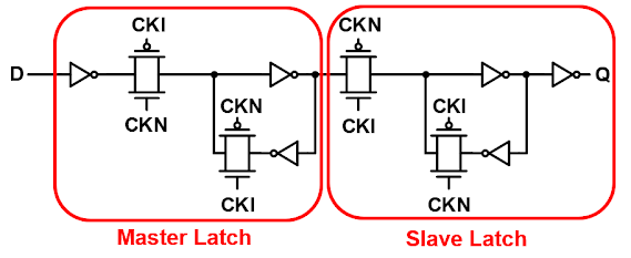
Transmission gates (TG) are a pair of pass transistors. The reason why TG is used instead of only one pass transistor is that a single pass transistor would pass a strong logic level and a weak level on the other. NMOS passes strong '0' and weak '1', whereas PMOS passes strong '1' and weak '0'. The first TG passes new data into the master latch (CK=0) while isolating the new data (D) from stored data in the master latch (CK=1). The second TG passes newly stored data in the master latch to the slave latch/output Q (CK=1) while isolating the new data (D) from passing to the output Q/the slave latch (CK=0). The third and fourth TGs are to loop (store) the data within the latch or release the latch contention when required.
The three inverters on these latches are mainly used for data buffering. The two inverters on the clock path as shown below are to generate clock transitions for controlling the timing of the fourth transmission gates (when to open, when to close).
How Flip-flop Works
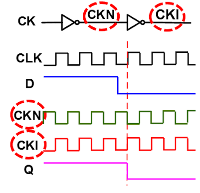
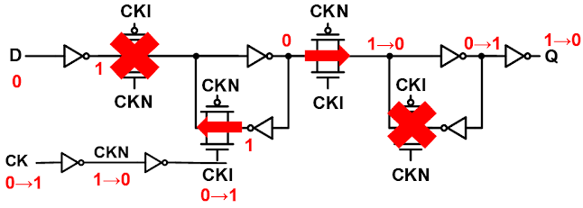
Now, jump into the detailed explanation of how this flip-flop works. Let's assume the old data stored inside the flip-flop is '1' and the new data (D) is '0'. How the flip-flop stores the new data '1' into its latches at the rising edge of the clock (CK) as shown in the waveform above.
When CK (clock) is LOW ('0')
When the clock is '0', CKN=1 and CKI=0. This turns the transmission gates TG1 ON and TG3 OFF. TG3 OFF releases the contention of the master latch while TG1 ON passes passing the new data '0' into the master latch. On the other hand, TG2 is switched OFF, isolating the newly stored data in the master latch from the slave latch, whereas TG4 is turned ON to keep the old data '1' in the slave latch.

↓

At the Rising Edge of the Clock ('0'→'1')
At the rising edge of the clock (0 → 1), CKN=1→0 and CKI=0→1. This will turn TG2 and TG3 ON while switching OFF TG1 and TG4. This keeps the newly stored data '0' in the master latch while passing the new data to the output Q/the slave latch. TG1 OFF isolates the input D from the master latch in order to prevent any changes in the input from affecting the data stored in the master latch.
↓

That's how the flip-flop works and stores data into its content. If you have any other questions, free to comment below.
To understand why setup and hold time are required in the flip-flop, read here.
To understand the setup time equations, check here.
Comments
Post a Comment