Last time, we described the reasons why setup and hold time are required in digital IC design. This article explained all the setup time equations and requirements for different timing paths in the digital IC design.
Setup time is the minimum time duration that the input data D required to be stable before the active clock edge so that the input data can be stored correctly into the flip-flop. Read more about setup time: here.
There are 3 main timing paths that require setup time constraints as shown below: register-to-register, input-to-register, and register-to-output.

Credit: Cadence Design Systems
Setup Time Equation for Register-To-Register Timing Paths
Most of the timing paths inside the chip are register-to-register. Setup time constraints ensure that the signal (Q) launched by the first flip-flop does not arrive too late so that the second flip-flop can capture it correctly.
Setup time equation for the reg-to-reg path:
Required Time = Clock Period - Setup Time (of the capturing flip-flop)
Arrival Time = CK→Q Delay (of Launching flip-flop) + Comb. Delay
To meet setup time constraint, Required Time ⋝ Arrival Time
=> Clock Period - Setup Time ⋝ CK→Q Delay (of Launching flip-flop) + Comb. Delay
=> Setup Time ≤ Clock Period - CK→Q Delay - Comb. Delay
Therefore, PnR Tools or Designers required to reduce the Comb. delay and CK→Q Delay of the flip-flop (swap flip-flop cell) OR increase the clock period (reduce clock frequency) to meet the setup time requirement. Another way to optimize is to swap the capturing flip-flop to another one with a smaller setup time constraint.

Credit: Cadence Design Systems
Setup Time Equation for Input-To-Register Timing Paths
Required Time = Clock Period - Setup Time (of Flip-Flop R2)
Arrival Time = CK→Q Delay (of flip-flop R1) + Comb. Delay 1 + Comb. Delay 2
As to be set in SDC Constraint, Input Delay = CK→Q Delay (of flip-flop R1) + Comb. Delay 1
Arrival Time = Input Delay + Comb. Delay 2
To meet setup time constraint, Required Time ⋝ Arrival Time
=> Clock Period - Setup Time (of Flip-Flop R2) ⋝ Input Delay + Comb. Delay 2
=> Setup Time (of Flip-Flop R2) ≤ Clock Period - Input Delay - Comb. Delay 2
Setup time equation for the input-to-register timing path suggests the same way of adjustment/optimization as the register-to-register path such as increasing the clock period, reducing input delay/comb. delay 2, and swapping flip-flop R2 with a smaller setup time requirement.

Credit: Cadence Design Systems
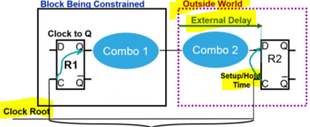
Setup Time Equation for Register-To-Output Timing Paths
Required Time = Clock Period - Setup Time (of flip-flop R2)
Arrival Time = CK→Q Delay (of flip-flop R1) + Comb. Delay 1 + Comb. Delay 2
External Delay is set in SDC constraint:
External Delay = Comb. Delay 2 + Setup Time (of flip-flop R2)
To meet setup time constraint, Required Time ⋝ Arrival Time
=> Clock Period - Setup Time (of flip-flop R2) ⋝ CK→Q Delay (of flip-flop R1) + Comb. Delay 1 + Comb. Delay 2
=> Setup Time (of flip-flop R2) ≤ Clock Period - CK→Q Delay (of flip-flop R1) - Comb. Delay 1 - Comb. Delay 2
Comments
Post a Comment